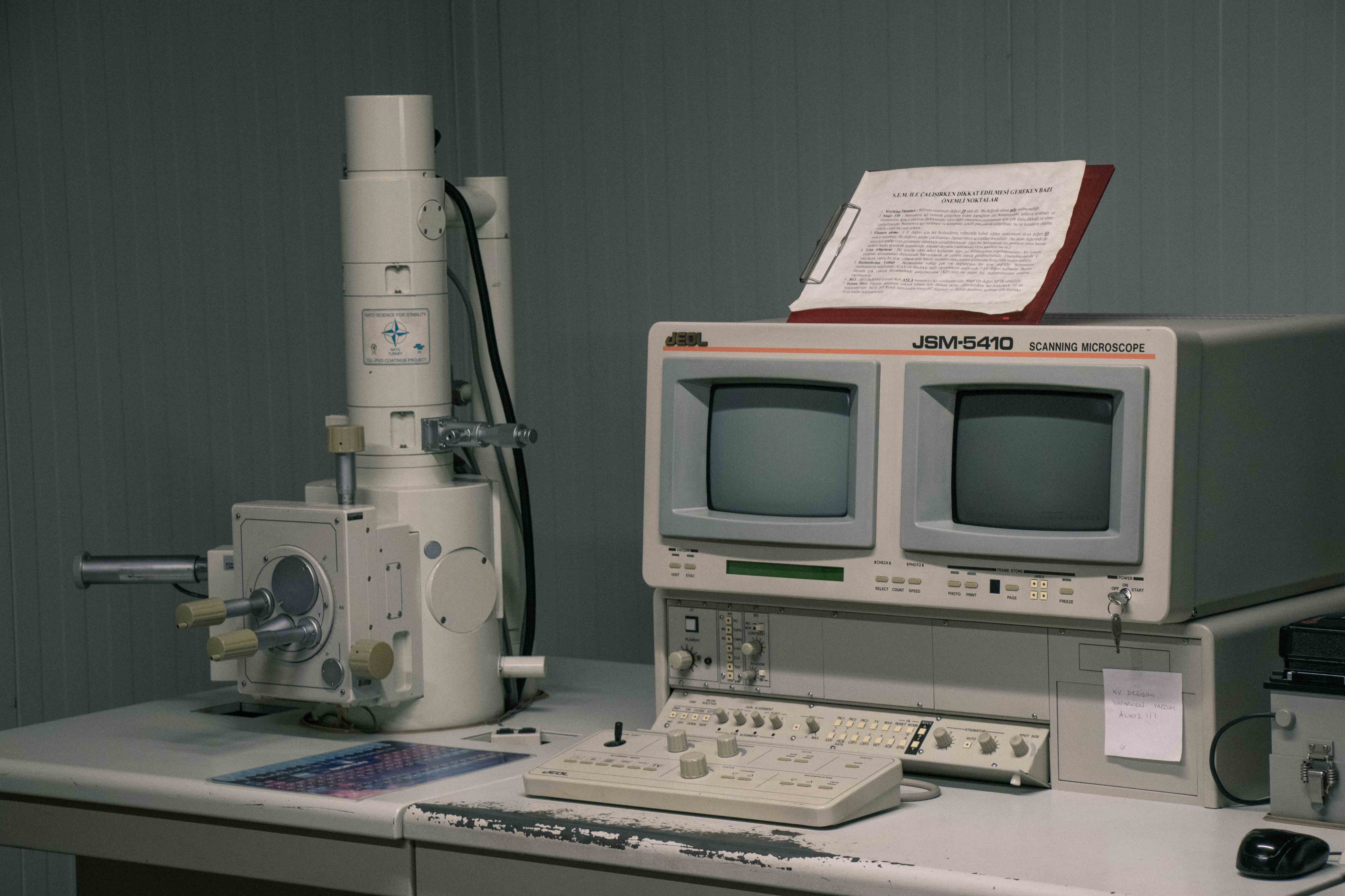
SEM-EDS sistemi, yüzey morfolojisini yüksek büyütmede görüntüler ve element analizi yapar.
|
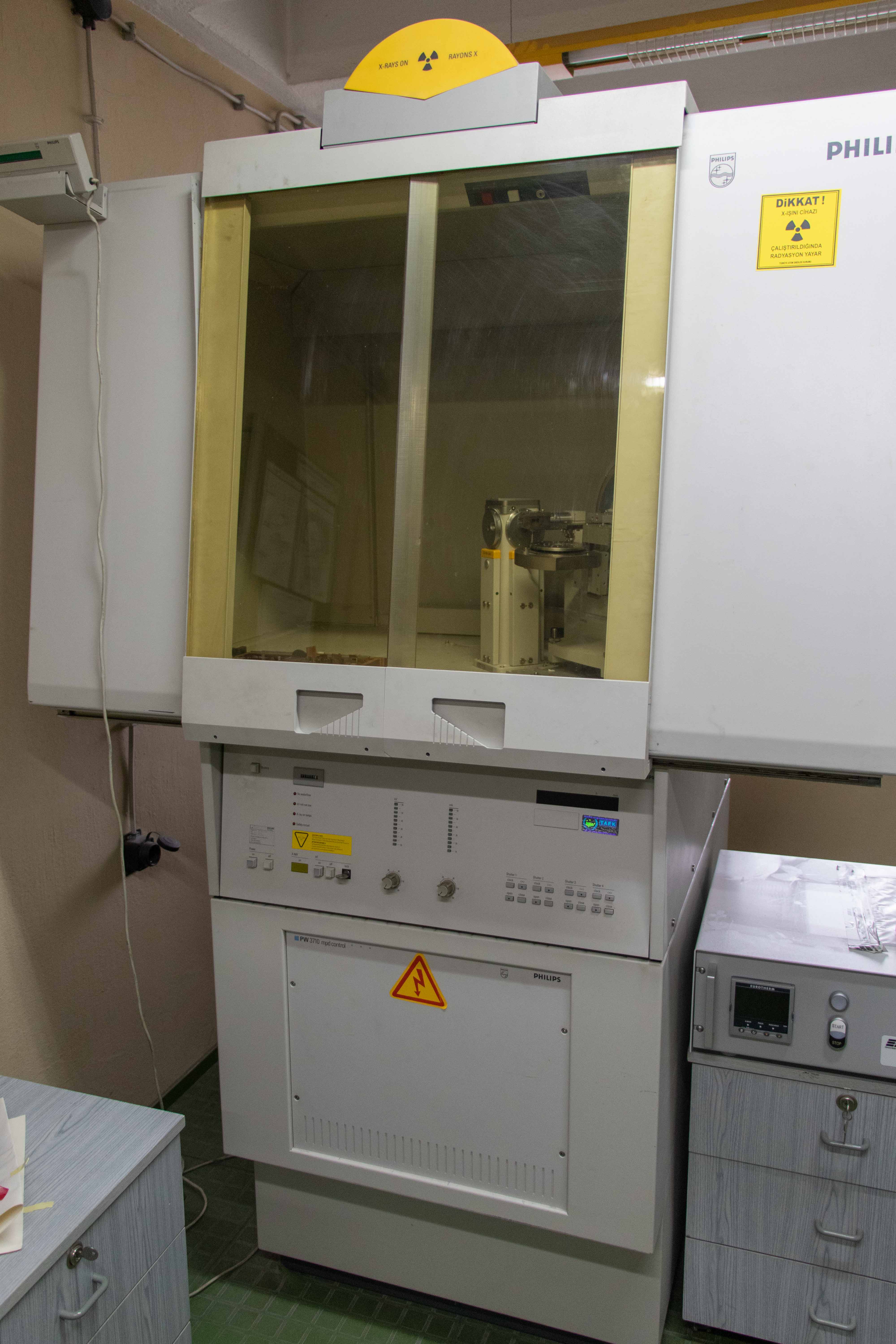
Cihaz |
SEM - Taramalı Elektron Mikroskobu |
|
Marka |
JEOL JSM 5410 |
Scanning Electron Microscope (SEM) is a type of electron microscope that produces images of a sample surface by scanning samples with a focused beam of electrons. The JEOL JSM-5410 SEM in our lab is capable of imaging sample surface morphologies by using secondary electrons or back-scattered electrons, equipped with an Energy Dispersive X-ray Spectrometer (EDS) for chemical analysis. With robust W filament, the SEM is capable of characterizing different materials.
- Resolution: 3.5 nm (Accv. 30 kV, WD = 6 mm, secondary electron image)
- Magnification: x15 (WD = 48 mm) to 200,000 (25 steps)
- Image modes:
– Secondary electron image (SEI) HV Mode
– Backscattered electron image (BEI) HV Mode
– Backscattered electron image (BEI) LV Mode
- Accelerating voltage: 0.5 to 30 kV
- EDAX Genesis Software: Point, line, and area EDS analysis as well EDS mapping
İlgili Rehberler
SEM-EDS Nasıl Yorumlanır?
Kaplama ve bozunma davranışını okumak için morfoloji ile bileşimi birlikte değerlendirin.
Yüzey Karakterizasyon Yöntemleri
Görüntüleme, kimya ve topografyayı birleştiren genel yorumlama çerçevesine geçin.
XPS Nedir?
Yüzeye duyarlı kimyasal analizlerin oksit tabakaları ve arayüzleri nasıl çözdüğünü görün.
XRD Nasıl Yorumlanır?
Kaplama yorumunu faz ve kristalografik bilgiyle destekleyin.
Profilometri Nedir?
Yükseklik haritalarından pürüzlülük yorumuna ve yüzey süreç kararlarına geçin.