SEM-Scanning Electron Microscopy is part of the Characterization Laboratory infrastructure at ITU Surface Lab. This page summarizes where the device sits in the laboratory workflow, what kind of measurements or process steps it supports, and why it matters in applied surface engineering studies.
In practice, the device is used to compare coating behavior, process stability, microstructural response, or surface-related performance outputs under controlled research conditions. The goal is not only to list the equipment, but to clarify the role it plays in experiment design and interpretation.
The summary, metadata cards, and detailed content below connect the device to real laboratory questions such as deposition strategy, corrosion response, tribological performance, characterization depth, or data reliability across projects and publications.
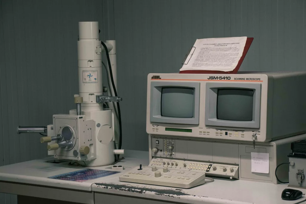
Equipment SEM-Scanning Electron Microscopy Brand JEOL JSM 5410 Scanning Electron Microscope (SEM) is a type of electron microscope that produces images of a sample surface by scanning samples with a focused beam of electrons. The JEOL JSM-5
|
Equipment |
SEM-Scanning Electron Microscopy |
|---|---|
|
Brand |
JEOL JSM 5410 |
Scanning Electron Microscope (SEM) is a type of electron microscope that produces images of a sample surface by scanning samples with a focused beam of electrons. The JEOL JSM-5410 SEM in our lab is capable of imaging sample surface morphologies by using secondary electrons or back-scattered electrons, equipped with an Energy Dispersive X-ray Spectrometer (EDS) for chemical analysis. With robust W filament, the SEM is capable of characterizing different materials.
- Resolution: 3.5 nm (Accv. 30 kV, WD = 6 mm, secondary electron image)
- Magnification: x15 (WD = 48 mm) to 200,000 (25 steps)
- Image modes:
– Secondary electron image (SEI) HV Mode
– Backscattered electron image (BEI) HV Mode
– Backscattered electron image (BEI) LV Mode
- Accelerating voltage: 0.5 to 30 kV
- EDAX Genesis Software: Point, line, and area EDS analysis as well EDS mapping
Related Guides
How to Interpret SEM-EDS
Tie morphology and composition together to read coatings and degradation behavior.
Surface Characterization Methods
Use the broader interpretation map that connects imaging, chemistry, and topography.
What Is XPS?
See how surface-sensitive chemistry helps interpret oxide layers and interfaces.
How to Interpret XRD
Use phase and crystallographic information to support coating interpretation.
What Is Profilometry?
Move from height maps to roughness interpretation and surface process decisions.